Author Affiliations
Abstract
1 Institute of Electromagnetics and Acoustics and Key Laboratory of Electromagnetic Wave Science and Detection Technology, Xiamen University, Xiamen 361005, China
2 Shenzhen Research Institute of Xiamen University, Shenzhen 518057, China
3 Department of Electrical Engineering, City University of Hong Kong, Hong Kong 999077, China
4 Institute of Materials Research and Engineering (IMRE), Agency for Science, Technology and Research (A*STAR), Singapore 138634, Singapore
5 Department of Materials Science and Engineering, National University of Singapore, Singapore 117575, Singapore
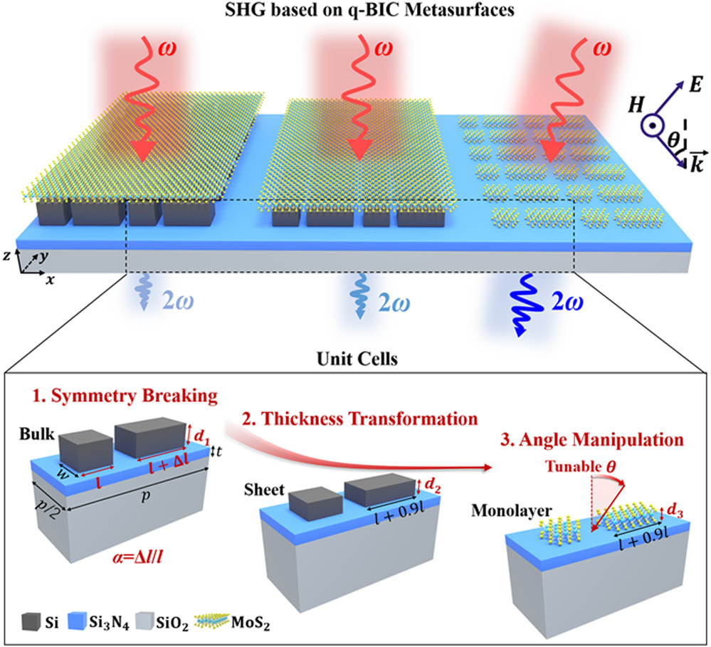
2D materials are promising candidates as nonlinear optical components for on-chip devices due to their ultrathin structure. In general, their nonlinear optical responses are inherently weak due to the short interaction thickness with light. Recently, there has been great interest in using quasi-bound states in the continuum (q-BICs) of dielectric metasurfaces, which are able to achieve remarkable optical near-field enhancement for elevating the second harmonic generation (SHG) emission from 2D materials. However, most studies focus on the design of combining bulk dielectric metasurfaces with unpatterned 2D materials, which suffer considerable radiation loss and limit near-field enhancement by high-quality q-BIC resonances. Here, we investigate the dielectric metasurface evolution from bulk silicon to monolayer molybdenum disulfide (), and discover the critical role of meta-atom thickness design on enhancing near-field effects of two q-BIC modes. We further introduce the strong-coupling of the two q-BIC modes by oblique incidence manipulation, and enhance the localized optical field on monolayer dramatically. In the ultraviolet and visible regions, the SHG enhancement factor of our design is times higher than that of conventional bulk metasurfaces, leading to an extremely high nonlinear conversion efficiency of 5.8%. Our research will provide an important theoretical guide for the design of high-performance nonlinear devices based on 2D materials.
Photonics Research
2024, 12(4): 784
Author Affiliations
Abstract
1 Institute of Electromagnetics and Acoustics and Key Laboratory of Electromagnetic Wave Science and Detection Technology, Xiamen University, Xiamen 361005, China
2 State Key Laboratory of Applied Optics, Changchun Institute of Optics, Fine Mechanics and Physics, Chinese Academy of Sciences, Changchun 130033, China
3 Terahertz Research Center, University of Electronic Science and Technology of China, Chengdu 610054, China
4 Microsystem and Terahertz Research Center, China Academy of Engineering Physics, Mianyang 621900, China
5 School of Physical Science and Technology and Institute of Theoretical and Applied Physics, Soochow University, Suzhou 215006, China
This publisher’s note corrects the funding order in
Photon. Res.10, 2836 (2022)10.1364/PRJ.472114.
Photonics Research
2023, 11(4): 581

Author Affiliations
Abstract
1 Institute of Electromagnetics and Acoustics and Key Laboratory of Electromagnetic Wave Science and Detection Technology, Xiamen University, Xiamen 361005, China
2 State Key Laboratory of Applied Optics, Changchun Institute of Optics, Fine Mechanics and Physics, Chinese Academy of Sciences, Changchun 130033, China
3 Terahertz Research Center, University of Electronic Science and Technology of China, Chengdu 610054, China
4 Microsystem and Terahertz Research Center, China Academy of Engineering Physics, Mianyang 621900, China
5 School of Physical Science and Technology and Institute of Theoretical and Applied Physics, Soochow University, Suzhou 215006, China
Terahertz (THz) molecular fingerprint sensing provides a powerful label-free tool for the detection of trace-amount samples. Due to the weak light–matter interaction, various metallic or dielectric metasurfaces have been adopted to enhance fingerprint absorbance signals. However, they suffer from strong background damping or complicated sample coating on patterned surfaces. Here, we propose an inverted dielectric metagrating and enhance the broadband THz fingerprint detection of trace analytes on a planar sensing surface. Enhancement of the broadband signal originates from the effects of evanescent waves at the planar interface, which are excited by multiplexed quasi-bound states in the continuum (quasi-BICs). One can evenly boost the near-field intensities within the analytes by tuning the asymmetry parameter of quasi-BIC modes. The multiplexing mechanism of broadband detection is demonstrated by manipulating the incident angle of excitation waves and thickness of the waveguide layer. Compared to the conventional approach, the THz fingerprint peak value is dramatically elevated, and the largest peak enhancement time is 330. Our work gives a promising way to facilitate the metasensing of the THz fingerprint on a planar surface and will inspire universal THz spectral analysis for trace analytes with different physical states or morphologies.
Photonics Research
2022, 10(12): 2836
1 青岛理工大学土木工程学院, 山东 青岛 266033
2 山东省高等学校蓝色经济区工程建设与安全协同创新中心, 山东 青岛 266033
为探索光纤布拉格光栅(FBG)传感技术在开口管桩贯入特性实验研究中的适用性,用一种增敏微型FBG应变传感器,对室内模型中开口管桩在沉桩过程中的受力状态进行了监测。研制了一种可拆卸的双壁开口模型管桩,将FBG传感器通过刻槽埋设和桩壁粘贴法安装在模型管桩上,测得模型管桩在贯入过程中的应力分布及变化规律。实验结果表明,该传感器配合特制的模型管桩,能满足开口管桩贯入特性的测试要求,且安装方便、存活率高。随模型管桩贯入深度的增加,开口管桩呈摩擦端承桩的承载特性,桩身内壁、外壁监测点处的轴力均增大,但各点增长速率存在差异;桩内壁、外壁侧摩阻力整体呈增大趋势,单位侧摩阻力出现不同程度的“退化效应”。
光纤光学 光纤布拉格光栅 应变传感器 模型管桩 监测 激光与光电子学进展
2020, 57(13): 130602
1 青岛理工大学土木工程学院, 山东 青岛 266033
2 山东省高等学校蓝色经济区工程建设与安全协同创新中心, 山东 青岛 266033
为了探索光纤布拉格光栅(FBG)传感技术在针对不同桩径静压桩贯入特性测试中的适用性,分别采用拉伸试验机、砂标法标定FBG应变传感器、FBG压力传感器,传感器线性度及测试精度较好,并配合不同桩径的模型桩在大尺寸模型箱中进行了室内静压沉桩试验。试验结果表明:FBG传感技术能够较好地满足不同桩径静压桩贯入特性的测试要求,所用传感器具有较高的线性度、灵敏性,经验证测试数据可靠,传感器安装方法可行;所用传感器能够对模型桩贯入过程中的压桩力、桩端阻力、侧摩阻力、桩身轴力、单位侧摩阻力进行动态、精准的监测,较为直观地反映了不同桩径的模型桩在静压过程中的贯入特性差异及变化规律。
测量 光纤布拉格光栅 传感器 静压桩 桩径 测试分析
采用相干态正交化法研究了非旋波近似下Tavis-Cummings(TC)模型中两非全同量子比特间的纠缠动力学问题, 分析了同一耦合强度下不同跃迁频率的量子比特和光场对两量子比特间纠缠演化的影响。研究结果表明, 在弱耦合情况下, 当其中一个量子比特的跃迁频率与光场频率相同而另一个量子比特的跃迁频率与光场频率对称失谐时, 量子比特间的纠缠完全相同; 当耦合强度较大时, 两对称失谐情况下的量子比特间的纠缠演化由于非旋波项的作用不再完全相同。
量子光学 量子纠缠 相干态正交化法 Tavis-Cummings模型 激光与光电子学进展
2018, 55(10): 102701
利用相干态正交化(ECS)法,讨论了两量子比特Rabi模型中的纠缠动力学问题,选取量子比特初态为交换对称的贝尔态,选取光场初态为真空态,分析了不同跃迁频率和不同光场-量子比特耦合强度下量子比特的纠缠演化特性。研究结果表明,在弱耦合情况下,当两个全同的量子比特的跃迁频率与光场频率的差值相同时,纠缠演化几乎相同;当非全同的量子比特跃迁频率相对光场频率对称失谐时,纠缠度比全同时大,失谐量越大,纠缠越强,且纠缠的变化周期与失谐量成反比。在共振情况下,当耦合强度不相等时,两量子比特纠缠演化存在主极大与次极大交替出现的现象;保持其中一个量子比特与光场的耦合强度不变,另一量子比特的耦合强度越强,次极大的峰值越大,但主峰峰值始终能达到最大纠缠;整个过程中纠缠演化表现出周期性。
量子光学 量子纠缠 相干态正交化 Rabi模型
西安工业大学电子信息工程学院,陕西 西安 710021
传统基于阵列的光源布局方式在室内难免存在光照度及系统误码率不均匀现象,为提高系统照度均匀性及通信可靠性,需合理对光源进行优化布局。本文以4 m×4 m×3 m的房间为模型,设计了单LED 阵列+灯带的环形光源布局模型。模型中间采用6×6 LED阵列,阵列内部灯珠之间的距离为0.3 m;四周采用环形灯带形式,灯珠个数为316 个,灯珠之间的距离为0.05 m。仿真结果表明,该模式下系统光照度均值为437.08 lx,光照度均匀性为93.9%,同时,系统误码率均值为2.8716×10⁻⁷。因此,本文所设计的环形光源布局模型兼顾了室内光照度分布的均匀性和通信的可靠性,可同时满足室内照明和通信,为室内可见光通信光源布局提供了一种优化方法。
可见光通信系统 光照度 误码率 阴影效应 visible light communication system light intensity bit error rate shadow effect


